
Taiwan’s Grand Process Technology targets panel
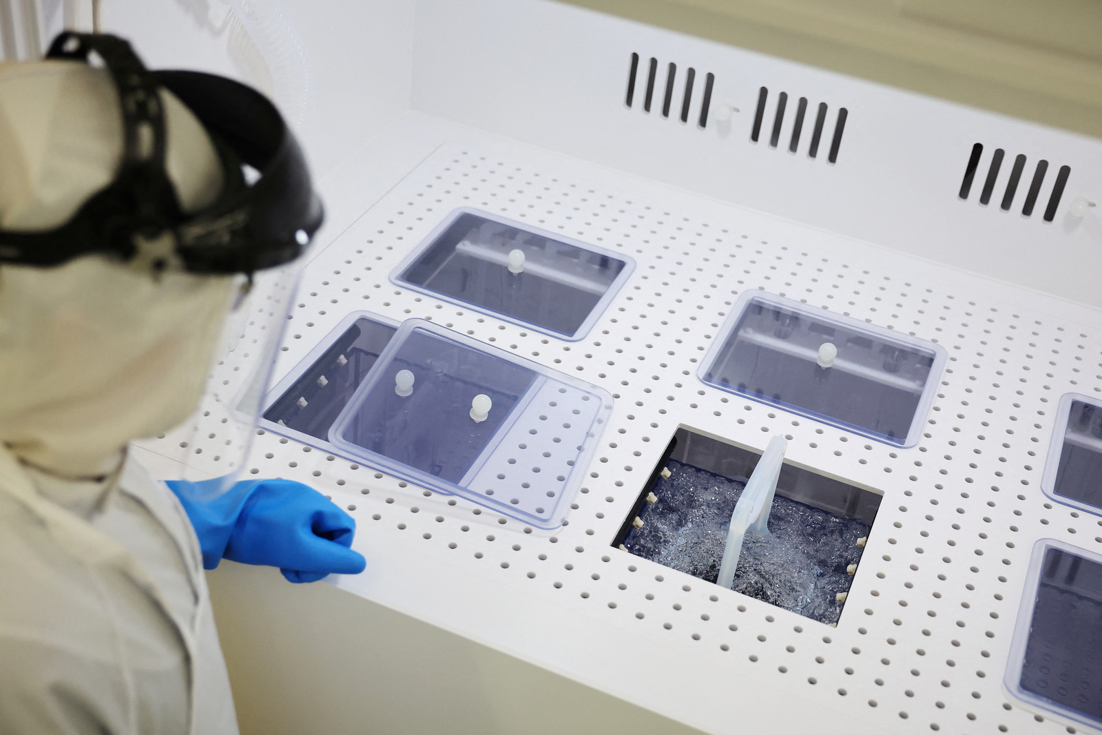
TAIPEI (Taiwan News) — Semiconductor equipment maker Grand Process Technology Corp. is expanding into panel-level packaging, a technology expected to play a growing role in advanced chip manufacturing.
The company will work with subsidiary Challentech International Corp. and German equipment maker Singulus Technologies to develop end-to-end process solutions for panel-level packaging, or PLP. Unlike traditional chip packaging, which uses round silicon wafers, PLP builds components on larger rectangular panels, potentially improving production efficiency and supporting higher computing performance, according to CTEE and Business Next.
Under the partnership, Grand Process Technology will contribute its expertise in semiconductor wet processes, which are used to clean and treat chip surfaces during manufacturing. Singulus will provide its large-scale physical vapor deposition technology, a vacuum-based coating process used to deposit thin layers of materials onto surfaces, according to Uanalyze and Ryh Shaun.
Challentech will support the project through semiconductor equipment distribution, technical services, and after-sales support. Singulus Co-CEOs Markus Ehret and Lars Lieberwirth said the partnership combines the companies’ strengths to deliver more complete and competitive packaging solutions.
The move comes as the semiconductor industry seeks new packaging technologies to support rising demand for AI-related computing power. Traditional wafer-based packaging has supported chip production for decades, but the growing complexity of AI chips has created new challenges.
As companies seek to integrate more components into a single package and improve data transfer speeds, unused space around the edges of round wafers and limits on larger chip packages have become increasingly important concerns. While PLP could help address these issues, the technology still faces several challenges.
One key issue is material and process compatibility, as larger panel sizes are more prone to deformation caused by thermal expansion and contraction. Another challenge is maintaining precise process control, especially for micrometer-level alignment. Improving yield rates is also critical, as instability at any stage of production could increase costs and delay deliveries.
Related Stories
 Technology
Ruanyun Edai Technology receives Nasdaq minimum bid price notice
1 hour ago
 Technology
Subnero Acoustic Modems Supported in OceanScan MST's LAUV
1 hour ago
 Technology
FlyDubai co
2 hours ago
 Technology
Meet the Islander who created technology that's in space right now
2 hours ago
 Technology
Commentator Katie Zacharia offered job of new White House press secretary
4 hours ago
 Technology
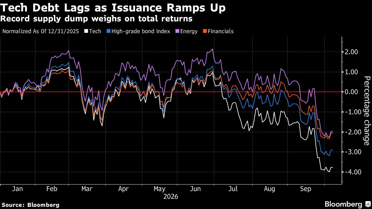
AI Debt Spree Hammers Tech Debt as Traders Rush to Reprice Risk
4 hours ago
 Technology
Genting, IOI Properties, PMB Technology, Press Metal, Unisem, EP Manufacturing, Astral Asia, Avangaad, Kinergy, Hektar REIT, and Ahmad Zaki
5 hours ago
 Technology
Trivolve Tech Launches IndianChain on Cardano Mainnet to Secure Agricultural Settlements
5 hours ago